From off-the-shelf AI cameras to fully custom machine vision systems — MVeeWorx delivers the hardware, software, and expertise to make your operations smarter.
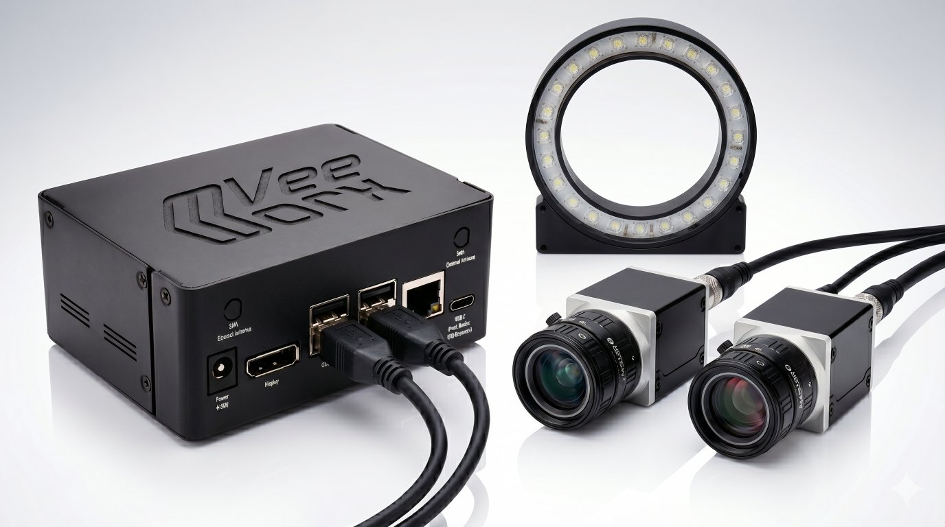
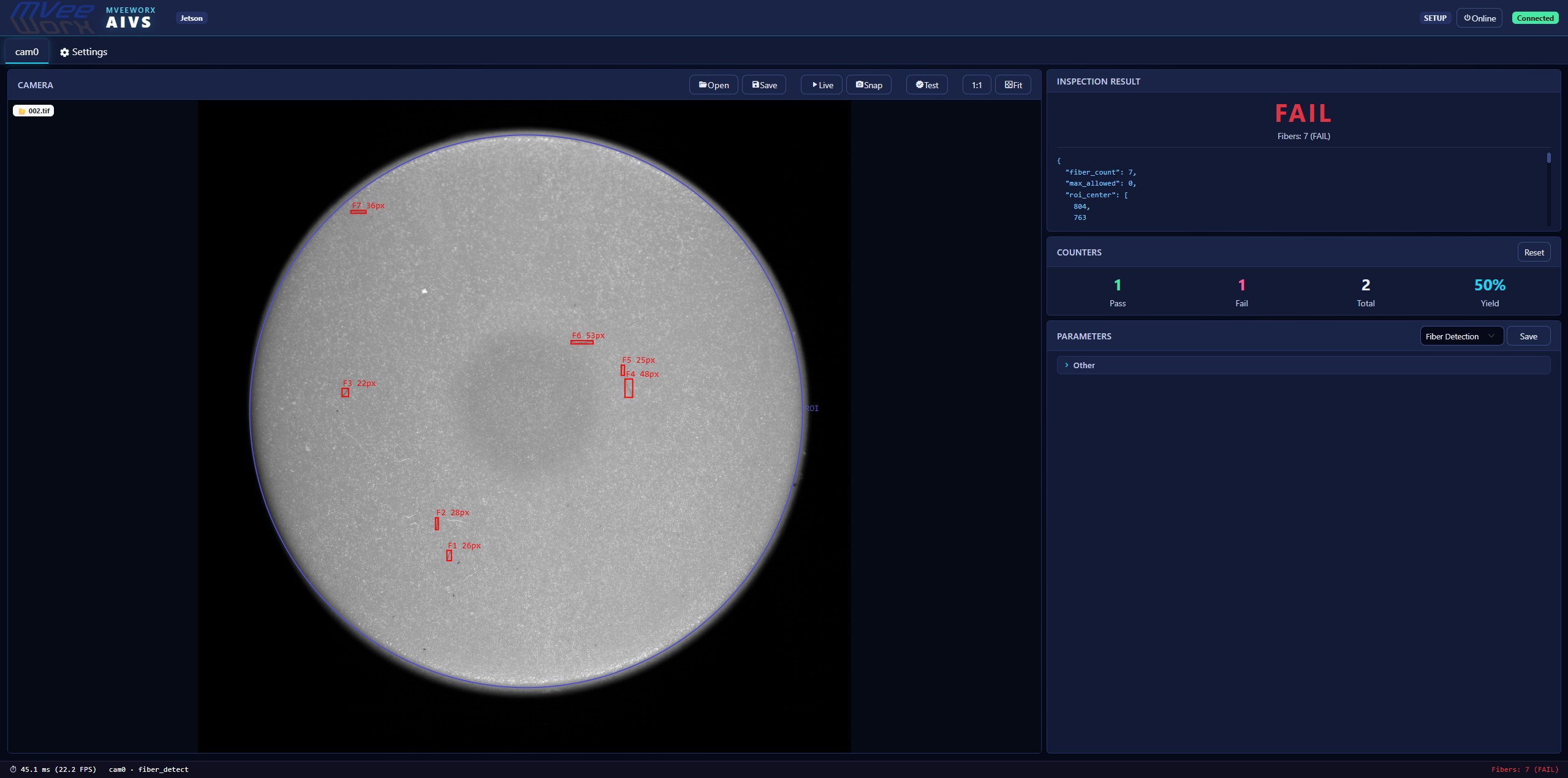
A compact, configurable edge AI inspection platform built around the NVIDIA Jetson Nano or Raspberry Pi 5 with AI HAT — paired with a user-selectable USB3 camera matched to your specific application. Everything runs on-device: no cloud dependency, no latency penalty, full data privacy.
Typical Applications
Over 25 years of hands-on machine vision experience — from optics and illumination design through to inspection algorithm development, software engineering, and production deployment.
We start by fully understanding your measurement or inspection challenge, then design a system architecture that is practical, cost-effective, and manufacturable — before any hardware is purchased.
Deep expertise in developing image processing and AI algorithms for real-world manufacturing inspection — including detection of defects that are invisible to the human eye.
End-to-end software engineering for machine vision applications — from camera acquisition and real-time image processing to operator interfaces and factory system integration.
A vision system is only as good as its deployment. We manage the full quality and commissioning process to ensure your system meets specification before it reaches your production floor.
A selection of production-deployed vision systems built from the ground up — from concept through to customer site.
Non-visible micro-crack detection system for solar wafers using specialised illumination and imaging techniques — catches defects invisible under standard lighting.
High-speed surface defect inspection covering the full wafer area — identifies stains, scratches, chipping, and contamination at production throughput rates.
Precision geometry measurement and full 3D surface profiling of solar wafers — edge/side inspection, bow, warp, and thickness variation measurement.
Automated inspection of IC packages — mold quality, lead coplanarity, marking verification — covering SOT, DDPAK, QFN, MLP, and other package types.
High-speed 3D wafer bump measurement using confocal microscopy — measuring ball height, coplanarity, and missing balls at throughput speeds demanded by production.
Laser-based 3D PCB solder paste inspection module — measuring paste volume, height, area, and offset to ensure reliable SMT assembly quality.
Our strongest experience is in high-volume manufacturing where measurement accuracy and system reliability are non-negotiable.
Crack detection, surface defect inspection, edge inspection, and 3D geometry measurement for solar wafer manufacturing lines.
Package inspection, 3D bump measurement, solder paste inspection, and surface defect detection across a wide range of IC package types.
PCB and component inspection — leadless packages, leaded components, tape-and-reel handlers — at the speeds required for high-volume SMT production.
Custom machine vision solutions for any automated production environment — from concept design and algorithm development through to full system deployment.
High-accuracy 3D measurement systems using confocal microscopy and laser triangulation — for dimensional gauging and surface profiling applications.
Bring us your inspection or measurement challenge — we will design a purpose-built system around your product, throughput, accuracy, and budget requirements.
Tell us about your application and we'll put together a tailored solution proposal — no obligation.